Self Assembly
Layer-by-Layer Nano Self-Assembly
Advantages
- New mechanical, electrical, optical, and catalytic properties
- Tunable material properties
- Biocompatibility
- Lager surface-to-volume ratio suitable for high-performance MEMS
- Unlimited coating cycles, controllable thickness, nanometer accuracy
- Substrates: silicon wafers, plastics, glass, etc.
- Assembled materials: polyions, charged nanoparticles, proteins, viruses, DNAs, etc.
- Simple fabrication steps and mild fabrication conditions
“Bottom-up” self-assembly of graphene may open a new way for M/NEMS with high performance and low cost.
Selective Publications
- M. Li, D. Mills, T. Cui, M. McShane, IEEE Trans. Nanobioscience, 4( 2), 2005: 170.
- F. Hua, T. Cui, et al., Nano Letters, 18, 4(5), 2004: 823.
- T. Cui, F. Hua, et al., US Patent No. 7,090,783.
- T. Cui, Y. Liu and M. Zhu, Appl. Phys. Lett., 87, 2005, p.183105.
- W. Xue, Y. Liu, and T. Cui, Appl. Phys. Lett., 89, 2006: 163512.
- W. Xue and T. Cui, IEEE MEMS Conference 2007.
Modified Lift-Off
Selective Publications
- M. Li, D. Mills, T. Cui, M. McShane, IEEE Trans. Nanobioscience, 4( 2), 2005: 170.
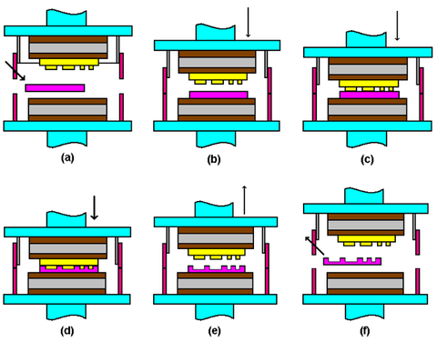
Hot Embossing Process
Advantages
- Low-cost method for high Volume production
- Raw materials are cheap
- Manufacturing is simple (batch replication)
- Compatible with the traditional IC processes
- Extremely precise
- Replications in nm-range are possible
- Thermal equilibrium process
- Homogeneous, low internal stress
- Very thin microstructures with high aspect ratios can be achieved
Selective Publications
Shrink Nanolithography
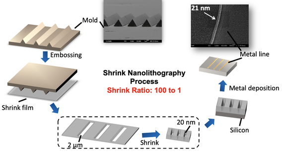
Shrink movable type nanolithography can produce patterns with a feature size of 20 nm or below at high throughput and low cost on wafer scale.
Selective Publications
- B. Zhang, M. Zhang, T. Cui, Applied Physics Letters, Vol. 100, 2012: 133113.


